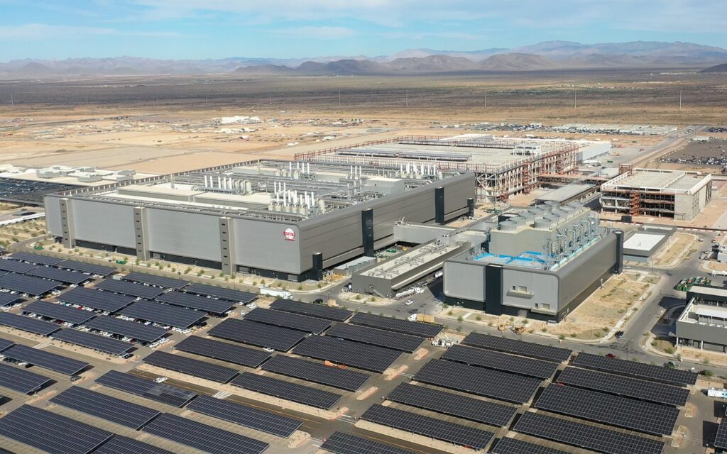
A Landmark Semiconductor Facility Highlights America’s Economic Paradox
In a bustling desert landscape near Phoenix, Arizona, a groundbreaking semiconductor manufacturing facility is taking shape, with the potential to redefine the global technology market. This ambitious project, spearheaded by Taiwan Semiconductor Manufacturing Company (TSMC), aims to produce cutting-edge chips on American soil for the first time.
TSMC, a titan in the semiconductor world, has committed to a multi-billion-dollar investment in its Arizona operations, motivated in part by the looming threat of tariffs on imports of chips. This facility, christened “Fab 21,” will play a crucial role in manufacturing advanced processors that power everything from smartphones to AI applications.
AMERICA FIRST: A Double-Edged Sword
President Trump has frequently spotlighted TSMC’s Arizona investment as a key victory in his “America First” agenda. “TSMC is the biggest there is,” he has declared, emphasizing the need for the U.S. to reclaim its position in the semiconductor industry, previously dominated by Taiwan and often seen as at risk due to geopolitical tensions with China.
The expansion, initially announced in March, signifies more than just a local economic boost; it carries weight in the ongoing U.S.-China competition. Trump sees this facility as a testament to his policies aimed at encouraging foreign companies to establish operations in the U.S. to mitigate tariff implications.
Guarded Innovations and Global Interdependence
The TSMC plant is notable not just for its promises of economic growth, but also for its stringent security measures. High-level innovations are closely protected, with the facility banning personal devices and written notes to prevent intellectual property theft. This emphasis on security reflects the importance of safeguarding the technology that underpins the world economy.
Greg Jackson, a facility manager, described the strategic efforts to maintain a sterile environment, crucial for the production of minuscule chips contained within advanced silicon wafers. This environment must be so clean that even a speck of dust could compromise the integrity of chip development.
Inside TSMC: The Future of Chips
Engineers are already making strides in chip production, with prototypes featuring “4 nanometre chips” that have the potential to contain trillions of transistors. The architecture of these chips represents the pinnacle of engineering sophistication, affirming that the production process involves thousands of meticulous steps.
The Broader Implications of the Arizona Fabrication Plant
While Trump credits his tariff threats for compelling TSMC’s investment, many industry speculators hint that this move was also strongly supported by the Chips Act introduced during Biden’s administration. This legislation aimed to bolster U.S. semiconductor manufacturing by funding research and providing incentives for domestic production.
Furthermore, TSMC’s operations illustrate the intricate global supply chain required for semiconductor production, underscoring that no single nation can independently manage the entire process. The company relies on materials and expertise from multiple countries, complicating the narrative of economic self-sufficiency.
| Aspect | Details |
|---|---|
| Location | Arizona, USA |
| Investment | $100 Billion |
| Target Chips | 4 nanometre Chips |
| Production Steps | 3,000 to 4,000 |
| Key Customers | Apple, Nvidia |
This factory encapsulates the paradox of Trump’s economic strategy: while it champions local manufacturing, it remains heavily reliant on a worldwide production network and innovations borne from international collaboration. As the technological arms race intensifies, the TSMC facility stands as a cornerstone for the future of chips and a testament to both the complexities of modern global trade and the geopolitical landscape.


